
The AI Inference Chip Landscape: 13 Architectures Competing With NVIDIA
Originally published on LinkedIn: August 1, 2026
Every company below is attacking the same two stages inside an LLM Inference, just from different angles. During inference, every user request consists of two distinct phases, each with very different hardware characteristics. NVIDIA GPUs, paired with software like TensorRT-LLM, vLLM, and SGLang, handle both stages competently. Every architecture below is betting that “competently” leaves room for a narrower, faster approach — usually by sacrificing generality for speed. Below is the core architectural bet behind each one.Groq — eliminate runtime decision-making
A GPU makes continuous scheduling decisions at runtime — what to fetch, what to execute next. Groq’s compiler makes all of those decisions ahead of time, so the hardware itself has no branch prediction, no caching, and no dynamic scheduling. Execution time becomes fully deterministic down to the clock cycle, which lets hundreds of chips synchronize without conventional networking overhead. The constraint is capacity: each chip carries only 230MB of SRAM, so large models require many chips working together. Best fit: real-time voice and agentic workloads, where consistent low latency matters more than raw throughput. Update (December 2025): NVIDIA agreed to a $20B non-exclusive license of Groq’s inference IP, and founder Jonathan Ross, president Sunny Madra, and much of the engineering team moved to NVIDIA. Groq continues to operate as an independent company under a new CEO, and GroqCloud keeps running without interruption, but the long-term roadmap for Groq-branded silicon is now tied to how NVIDIA chooses to integrate the LPU architecture into its own inference stack. Analysts have framed this as a template NVIDIA may repeat with other inference-specialist challengers rather than a one- off deal.Cerebras — collapse the chip boundary entirely
Rather than dicing a silicon wafer into hundreds of individual chips, Cerebras keeps the full wafer as a single processor, with 44GB of on-chip SRAM and roughly 21 PB/s of internal bandwidth. Because both prefill and decode execute on the same wafer, there’s minimal off-chip data movement. Best fit: long-context training and low-latency inference for models that fit within its on-wafer memory; less efficient once a model must be partitioned across multiple wafers. Update (2026): Cerebras signed a multi-year partnership with AWS, marking the first time a major hyperscaler has hosted Cerebras hardware inside its own data centers. The deployment uses AWS Trainium3 for prefill and Cerebras CS-3 systems for decode, delivered through Amazon Bedrock — the same GPU-plus- specialist disaggregation pattern discussed earlier in this piece, now running at hyperscale. Cerebras also signed a separate multi-year agreement with OpenAI (reportedly over $20B, covering roughly 750MW of inference capacity), reinforcing that its commercial traction is currently concentrated in decode-heavy, latency-sensitive serving rather than displacing GPUs for training.SambaNova — treat the model as a continuous dataflow graph
GPUs execute a model as a sequence of discrete kernels, each requiring synchronization before the next begins. SambaNova’s compiler instead maps the entire computation graph spatially across compute and memory units, so intermediate data flows directly between stages without returning to memory. A three-tier memory hierarchy (SRAM/HBM/DDR) also lets it keep large Mixture-of-Experts libraries resident at low cost, loading only the active experts into faster memory. Best fit: large MoE models; one of the more production-mature non-GPU platforms in this group.d-Matrix — perform computation inside the memory array
Conventional architectures move weights from memory into separate compute units for every operation. d-Matrix’s Corsair places digital multipliers directly within the SRAM structures that store the weights, so computation happens where the data already resides, substantially reducing data movement. Its fast on-chip memory is limited (roughly 16GB), so larger models rely on external LPDDR for capacity. Best fit: decode, particularly in heterogeneous deployments where a GPU handles prefill and Corsair handles decode — a pattern already being tested in production. Note on Microsoft: Microsoft’s venture arm, M12, is an investor in d-Matrix, and d-Matrix has used Azure-hosted EDA tooling during chip development — a financial and infrastructure relationship, not a native Azure accelerator SKU or Marketplace listing. As of this writing there is no public evidence of Corsair being offered as an Azure instance type.MatX — a programmable accelerator built exclusively for large transformers
Designed by former Google TPU engineers, MatX removes the general- purpose hardware a GPU carries for graphics and non-AI workloads, while remaining fully programmable. Weights typically reside in SRAM for low- latency reuse; the KV cache, which grows dynamically, is stored in HBM. It targets training, reinforcement learning, prefill, and decode on a single platform. Best fit: large dense and MoE models across both training and inference — architecturally broad, though independent benchmarks remain limited.Etched — fix the transformer execution path in silicon
Etched’s Sohu chip hardwires the transformer operations themselves — attention, matrix multiplication, layer normalization — directly into the circuit, eliminating the instruction-fetch and scheduling overhead a GPU requires for each step. It is not tied to one model’s weights; it can load different transformer models, provided their operations map onto its supported datapath. Best fit: large-scale transformer serving, contingent on transformers remaining the dominant model architecture.Taalas — fix both the architecture and the trained weights in silicon
Taalas extends the same idea further than Etched: it compiles a specific model, including its trained parameters, directly into the chip. During decode, there are no weights to fetch from external memory at all, since they are physically embodied in the circuit. Best fit: a single, extremely stable model served at very high volume. The risk is proportionally high — a newer model cannot be loaded without new silicon.Rebellions — a conventional but inference-optimized accelerator
This is the least specialized architecture in the group. Rebellions retains a familiar structure — SRAM, HBM, compute engines, a compiler — but removes hardware unrelated to inference and supports mixed precision (FP8/FP16/INT4). It is architecturally closer to a Google TPU or AWS Inferentia than to the memory-centric designs above. Best fit: balanced enterprise inference; the strongest deployment evidence currently comes from Korean telecom and sovereign-AI partnerships.Positron — maximize realized memory bandwidth rather than peak bandwidth
Positron’s premise is that GPUs rarely use the HBM bandwidth they already have during decode, due to irregular access patterns. Atlas, its current FPGA-based system, is designed around predictable transformer memory access and reports roughly 93% realized bandwidth utilization. Its successor, Asimov, replaces HBM with large-capacity LPDDR5X to hold larger models per accelerator at lower cost. Best fit: memory-bound decode workloads at a lower cost basis than HBM-based systems; Atlas already has disclosed deployments, including Cloudflare and Parasail.Axelera — compute-in-memory, positioned for the edge
Architecturally similar to d-Matrix — digital compute performed within SRAM — but initially targeted at edge vision, robotics, and video analytics rather than data-center inference. Newer platforms (Europa, and the planned Titania) are extending toward compact language and vision- language models, with data-center-class inference still on the roadmap. Best fit: edge and vision workloads today; not yet a direct comparison point for data-center LLM serving.Tensordyne — replace multiplication with addition
Tensordyne represents numbers logarithmically, using the identity log(a×b) = log(a) + log(b) to replace hardware multipliers with simpler adders, which require less silicon area and power. The freed die area is allocated to additional SRAM and compute. The tradeoff is that operations transformers rely on heavily — residual additions, softmax, normalization — become more complex to perform accurately in logarithmic form. Best fit: potentially both prefill and decode, including MoE routing; the architecture has taped out but remains unproven at production scale.Fractile — near-total in-memory execution
Fractile claims that approximately 99.99% of inference operations execute directly within on-chip memory, with RISC-V vector processors handling the remainder. Conceptually adjacent to d-Matrix, but Fractile has disclosed considerably less about its implementation. Best fit: decode- bound inference, in principle; current performance claims should be treated as targets rather than measured results.Olix — connect distributed SRAM using photonic interconnect
Olix’s premise is that SRAM offers the best latency characteristics for inference, but no single chip can hold enough of it for a large model. Its approach is to distribute memory and compute across many SRAM-based chips and connect them optically rather than electrically, since photonic links scale bandwidth more efficiently over distance than copper. Based on current disclosures, the photonics serve as interconnect rather than performing the matrix computation itself. Best fit: rack-scale decode, in theory — this remains the least disclosed architecture in the group, closer to a technical thesis than a benchmarked product.Quick-Reference Summary
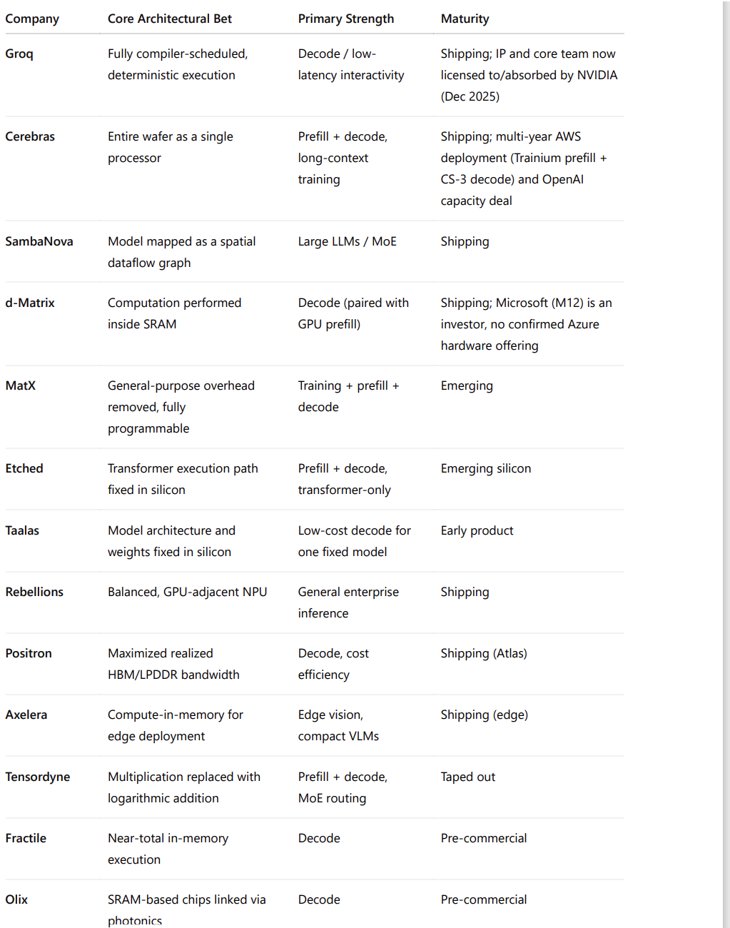
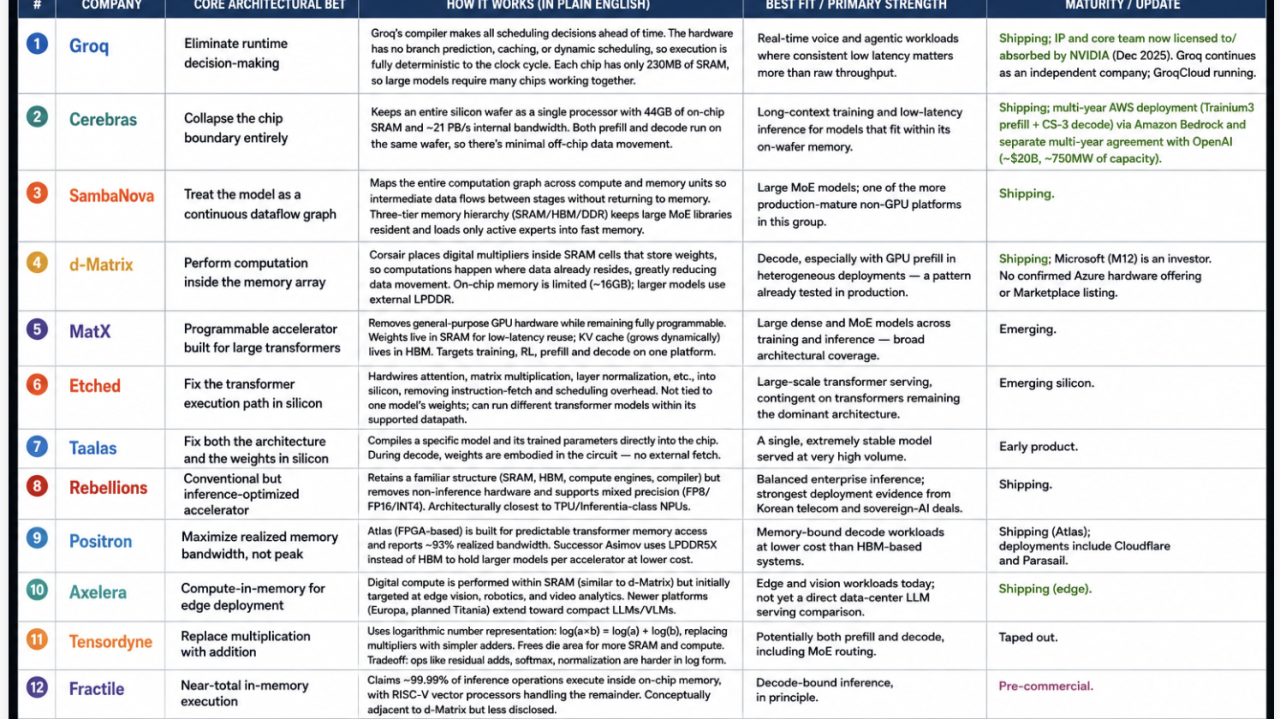
Here’s the combined table with all 13 AI inference architectures in one format that you can copy directly into Word, Markdown, or Excel.